
Memory Hierarchy
1. MEMORY HIERARCHY
MEMORY HIERARCHY
3.0 INTRODUCTION
Some programs on your computer open instantly, while others require a few seconds to launch. This occurs due to the existence of various types of memory in computers, each operating at distinct speeds. This concept is referred to as the memory hierarchy. The memory hierarchy of a computer systematically arranges memory components from the fastest and most costly, such as CPU registers and cache, to the slowest yet largest, including hard drives and SSDs. The system enhances computational efficiency by positioning frequently accessed data in proximity to the processor while relegating less utilized data to more distant storage. A computer organizes data similarly to how one might store snacks: frequently accessed data is readily available, less-used data is stored in secondary locations, and bulk data is kept in primary storage.
3.1 Control Points and the Generation of Control Signals (Hardwired vs Microprogrammed Control Units)
In a computer, a control point refers to a specific location or component (like a register, ALU, memory, bus, etc.) that can be controlled using electrical signals during the execution of an instruction. Control points is just like switches or knobs that the control unit turns ON or OFF to make sure the right operations happen at the right time.
For example: To move data from register A to register B, a control signal must:
* Enable register A to put its data on the bus.
* Enable register B to read data from the bus.
These ON/OFF signals are called control signals, and they are generated by the control unit of the CPU.
How are Control Signals Generated?
Control signals can be generated in two major ways:
1. Hardwired Control Unit: This approach uses fixed logic circuits to directly generate control signals. It's like a complex network of digital components (gates, flip-flops, decoders) wired together to respond to instruction codes. Each instruction has a binary opcode. This opcode enters a decoder which activates the correct set of control signals needed for that instruction. These signals control ALU operations, memory reads/writes, data transfers, etc. Hardwired Control Unit is fast and efficient which makes the performance better and is good for simple or reduced instruction set computers (RISC). However, hardwired control unit is not flexible i.e; changes require hardware modification and also, its complex logic becomes harder to manage as instruction set grows
2. Microprogrammed Control Unit: Uses software-like instructions called microinstructions which are stored in a control memory. Each microinstruction tells the control unit what control signals to activate. When an instruction is fetched, the control unit goes to the control memory to find a microprogram for that instruction. The microprogram is a sequence of microinstructions.
Each microinstruction sets the control points for one small operation. Microprogrammed control unit is easy to modify (just change the microprogram, not the hardware). In addition, Microprogrammed control unit is easier to implement complex instruction sets (like in CISC processors). Nevertheless, Microprogrammed control unit is slower than hardwired control (since it needs to read from control memory).
3.2 Memory Hierarchy
In computer architecture, memory hierarchy refers to the structured arrangement of different types of memory/storage in a system based on speed, size, and cost. That is; from fastest to slowest:
Registers > L1 Cache > L2 Cache > L3 Cache > Main Memory (RAM) > Secondary Storage (SSD/HDD)
The memory hierarchy of a computer system is an ordering of memory components in an increasing order of size and response time. this is shown in Figure 3.1.
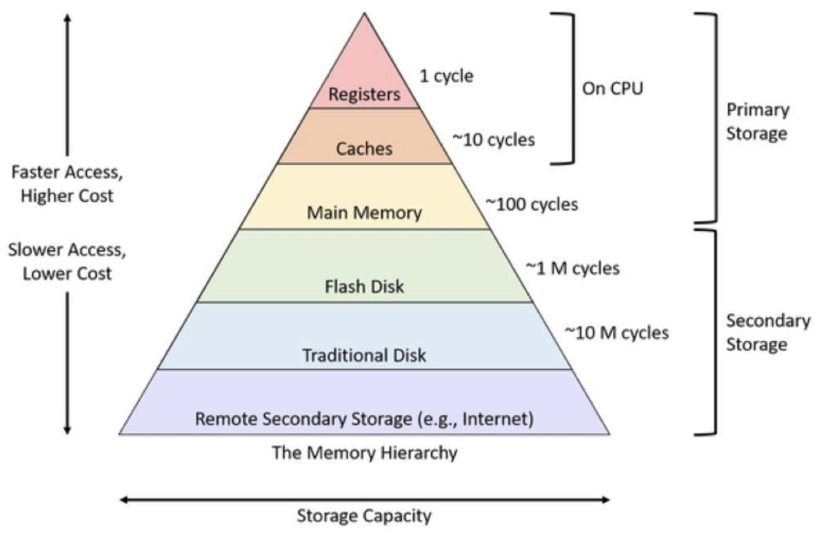
Figure 3.1: Memory Hierarchy.
In computer architecture, a word is a unit of data of a defined bit length that can be addressed and moved between storage and the computer processor. Usually, the defined bit length of a word is equivalent to the width of the computer's data bus so that a word can be moved in a single operation from storage to a processor register as showed in Figure 3.2. For any computer architecture with an eight-bit byte, the word will be some multiple of eight bits. In IBM's evolutionary System/360 architecture, a word is 32 bits, or four contiguous eight-bit bytes. In Intel's PC processor architecture, a word is 16 bits, or two contiguous eight-bit bytes.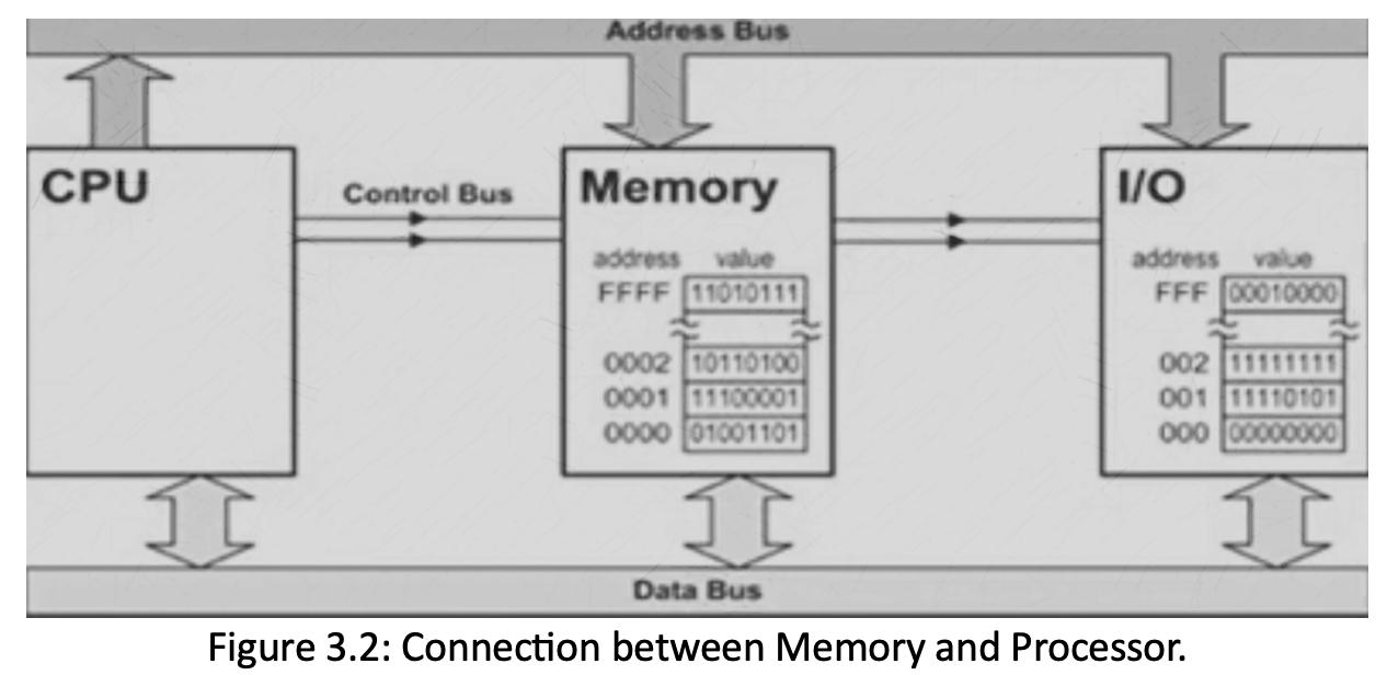
The connection between memory and processor is through the various buses. Such as:
i. Address Buss (AB): is unidirectional (one direction) because address flow in one direction from processor to memory or from processor to input/ output devices. The width of AB determines the amount of physical memory addressable by the processor.
ii. Data Bus (DB): Is bidirectional (two direction) because allow data to transfer between the processor (CPU) and memory (RAM). The width of DB indicates the size of the data transferred between the processor and memory or I/O device.
iii. Control Bus (CB): is bidirectional (two direction) used by CPU for communicating with other devices within the computer. It carries control signals from CPU .The typical control signals ,include memory read, memory write, I/O read, I/O write, bus request. These control signals indicate the type of action taking place in the computer system.
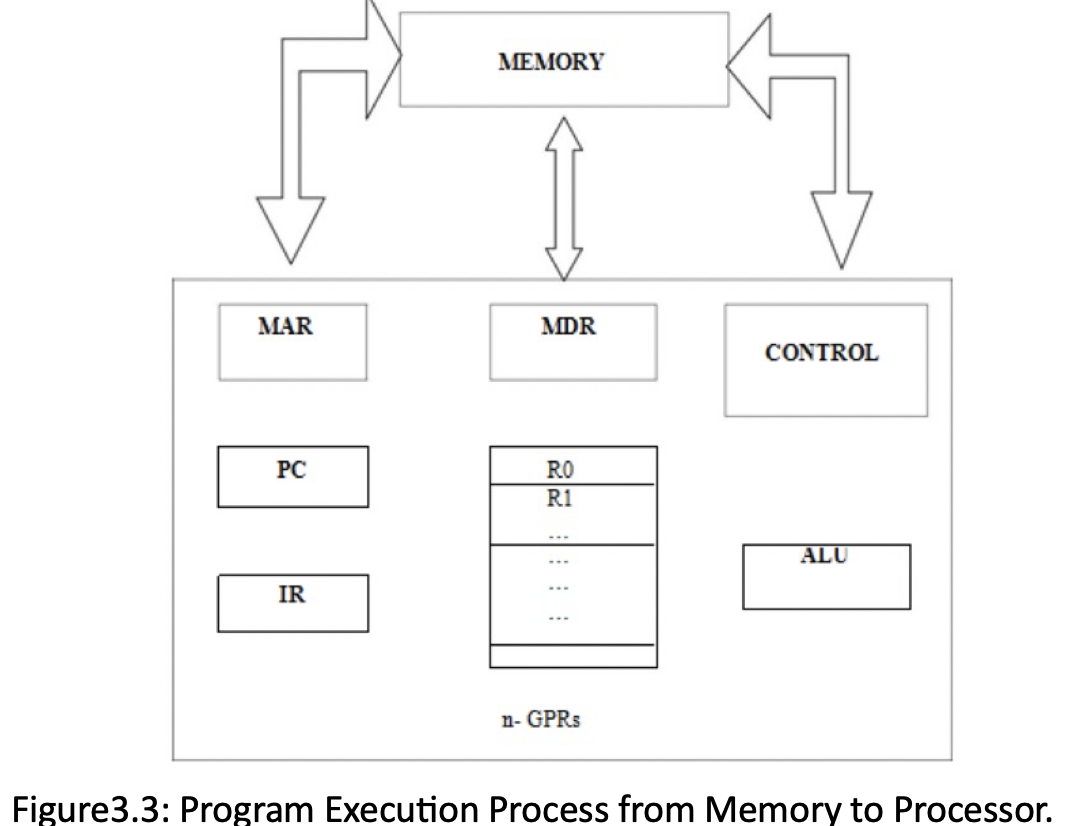
To provide easy access to a word in memory, a distinct address is associated with each word location. Addresses are numbers that identify memory location. Number of bits in each word is called word length of the computer. Programs must reside in the memory during execution. Instructions and data can be written into the memory or read out under the control of processor. Memory in which any location can be reached in a short and fixed amount of time after specifying its address i. e. RAM as illustrated in Figure 3.3.
The time required to access one word in called Memory Access Time. Memory which is only readable by the user and contents of which can’t be altered is called read only memory (ROM) it contains operating system.
• Memory Circle Time is the minimum time between start of two operations and is generally measured in Nanoseconds.
• The instruction register (IR) holds the instructions that are currently being executed. Its output is available for the control circuits which generates the timing signals that control the various processing elements in one execution of instruction.
• The program counter PC is a specialized register that keeps track of execution of a program. It contains the memory address of the next instruction to be fetched and executed. The instruction registers (IR): - Holds the instructions that are currently being executed. Its output is available for the control circuits which generates the timing signals that control the various processing elements in one execution of instruction. Besides IR and PC, there are n-general purpose registers R0 through Rn-1.
• MAR (Memory Address Register) holds the address of the location to be accessed.
• MDR (Memory Data Register) contains the data to be written into or read out of the address location.
1. Cache Memory: Cache is a small, fast memory located inside or close to the CPU. It stores copies of frequently accessed data. When the CPU needs data, it first checks the cache as illustrated in Figure 3.4:
If the data is found → it's a cache hit (very fast!)
If not → cache miss (CPU goes to slower main memory)
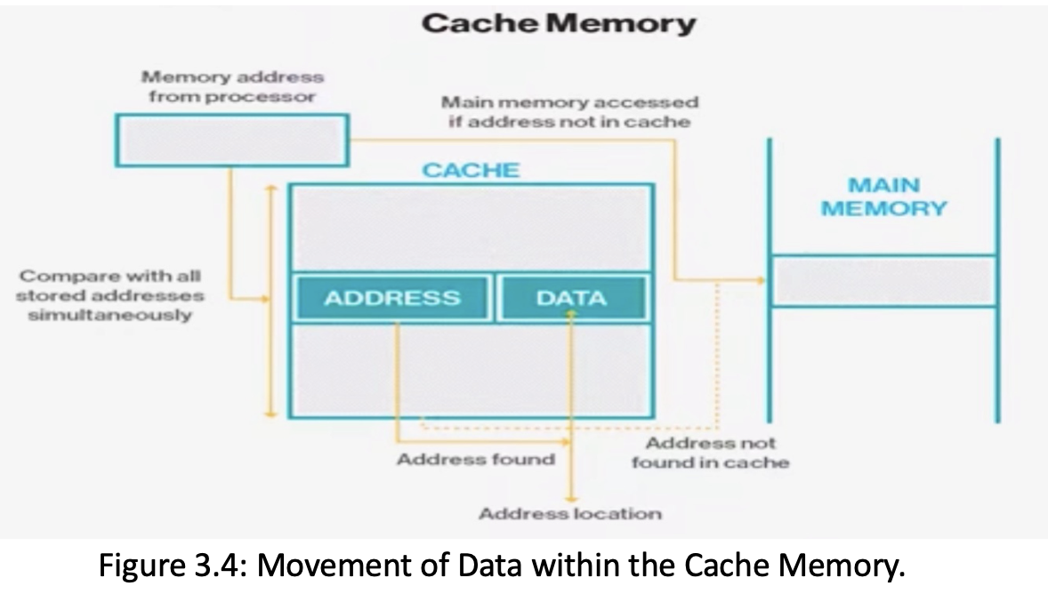
The Cache memory is responsible for storing frequently used instructions and data. The CPU first looks to access frequently/ commonly used data in this component before going down the memory hierarchy.
Temporal locality: recently accessed data is likely to be used again soon.
Spatial locality: data near recently accessed data is likely to be used. Cache takes advantage of this, reducing how often the CPU must wait for slow memory. Most common Cache memory include: L1, L2 and L3 (Sometimes up to L4 in some processors):
L1 is the fastest to access (usually very small) and is usually embedded in the microprocessor.
L2 is larger but slower to access and is usually located on a separate chip independent from the microprocessor.
L3 is largest but slowest to access and is usually located on a separate chip independent from the microprocessor similar to L2.
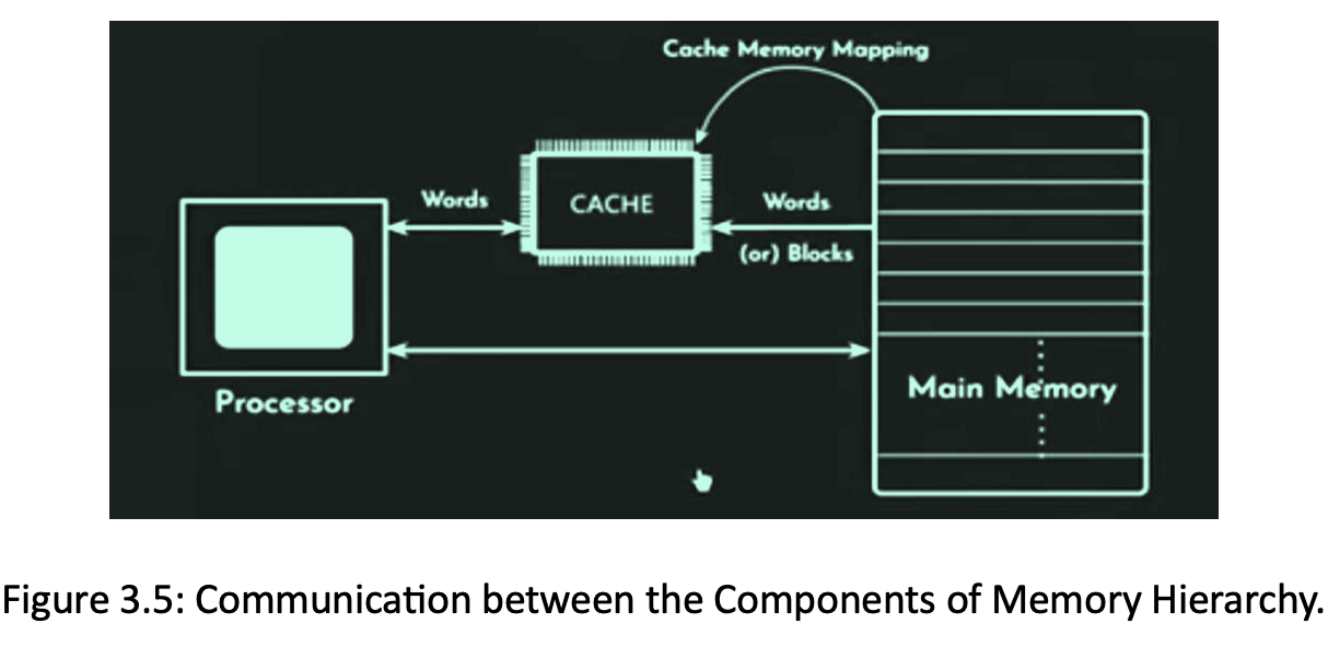
2. Main memory (DRAM) is a component of memory that stores the data in memory cells. It is a temporary storage- it stores the data needed by programs that are running, but when you exit the programs, the memory responsible for running those programs in the DRAM gets cleared. This is demonstrated using the diagram in Figure 3.5.
3. Secondary Memory (such as Hard drive and Magnetic tape) is a memory component that permanently stores data in the memory. Memory from hard disk is not directly accessed by the CPU, hence, it is slower compare to DRAM but cheaper. In addition, it is often used for backing up large data. Usually, data are stored on the disks or tapes connected by networks such as cloud.
3.3 Virtual Memory: gives the illusion that we have more RAM than we really do. It uses disk space (e.g., SSD) to temporarily store parts of programs or data not actively in use. The OS divides memory into pages. When data not in RAM is needed, it’s swapped in from disk. This process is managed through page tables and Memory Management Unit (MMU). MMU allows large applications to run smoothly even with limited RAM and also keeps the CPU working with what’s important, not everything at once.